- 您现在的位置:买卖IC网 > Sheet目录356 > SI8423BD-B-IS (Silicon Laboratories Inc)ISOLATOR 2CH 5KV 150M 16SOIC
�� �
�
�Si8410/20/21� (5� kV)�
�Si8� 422/23� (� 2.� 5� &� 5� k� V)�
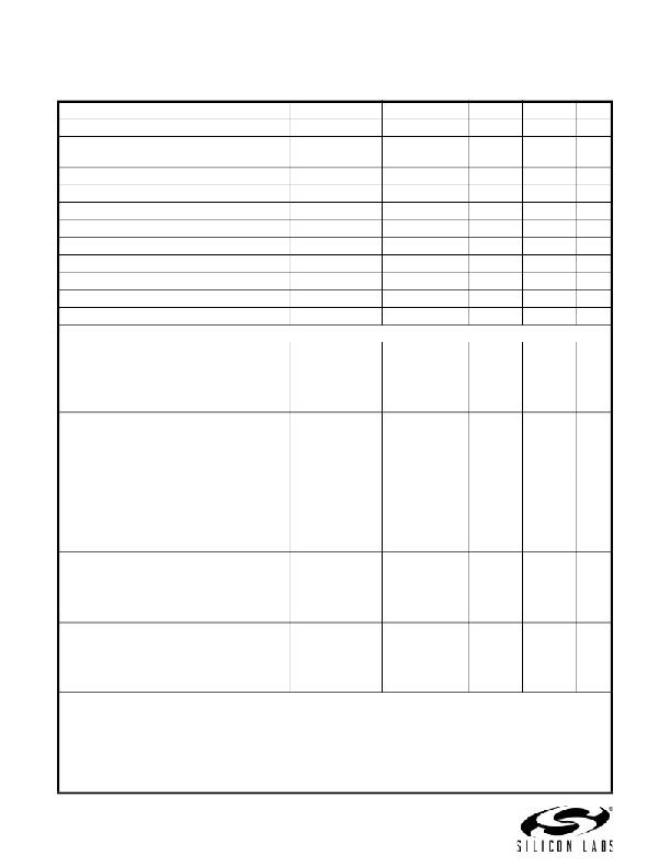
�Table� 2.� Electrical� Characteristics�
�(V� DD1� =� 3.3� V� ±10%,� V� DD2� =� 3.3� V� ±10%,� T� A� =� –40� to� 125� °C)�
�Parameter�
�Symbol�
�Test� Condition�
�Min�
�Typ�
�Max�
�Unit�
�VDD� Undervoltage� Threshold�
�VDD� Negative-Going� Lockout�
�VDDUV+� V� DD1� ,� V� DD2� rising�
�VDD� HYS�
�2.15�
�45�
�2.3�
�75�
�2.5�
�95�
�V�
�mV�
�Hysteresis�
�Positive-Going� Input� Threshold�
�Negative-Going� Input� Threshold�
�Input� Hysteresis�
�High� Level� Input� Voltage�
�Low� Level� Input� Voltage�
�High� Level� Output� Voltage�
�Low� Level� Output� Voltage�
�Input� Leakage� Current�
�VT+�
�VT–�
�V� HYS�
�V� IH�
�V� IL�
�V� OH�
�V� OL�
�I� L�
�All� inputs� rising�
�All� inputs� falling�
�loh� =� –4� mA�
�lol� =� 4� mA�
�1.6�
�1.1�
�0.40�
�2.0�
�—�
�V� DD1� ,V� DD2� –� 0.4�
�—�
�—�
�—�
�—�
�0.45�
�—�
�—�
�3.1�
�0.2�
�—�
�1.9�
�1.4�
�0.50�
�—�
�0.8�
�—�
�0.4�
�±10�
�V�
�V�
�V�
�V�
�V�
�V�
�V�
�μA�
�Output� Impedance�
�(Si8410/20)� 1�
�Z� O�
�—�
�50�
�—�
�?�
�DC� Supply� Current� (All� inputs� 0� V� or� at� supply)�
�Si8410Ax,� Bx�
�V� DD1�
�All� inputs� 0� DC�
�—�
�1.0�
�1.5�
�V� DD2�
�V� DD1�
�V� DD2�
�All� inputs� 0� DC�
�All� inputs� 1� DC�
�All� inputs� 1� DC�
�—�
�—�
�—�
�1.0�
�3.0�
�1.0�
�1.5�
�4.5�
�1.5�
�mA�
�Si8420Ax,� Bx�
�V� DD1�
�All� inputs� 0� DC�
�—�
�1.3�
�2.0�
�V� DD2�
�V� DD1�
�V� DD2�
�All� inputs� 0� DC�
�All� inputs� 1� DC�
�All� inputs� 1� DC�
�—�
�—�
�—�
�1.7�
�5.8�
�1.7�
�2.6�
�8.7�
�2.6�
�mA�
�Si8421Ax,� Bx�
�V� DD1�
�All� inputs� 0� DC�
�—�
�1.7�
�2.6�
�V� DD2�
�V� DD1�
�V� DD2�
�All� inputs� 0� DC�
�All� inputs� 1� DC�
�All� inputs� 1� DC�
�—�
�—�
�—�
�1.7�
�3.7�
�3.7�
�2.6�
�5.6�
�5.6�
�mA�
�Si8422Ax,� Bx�
�V� DD1�
�All� inputs� 0� DC�
�—�
�3.7�
�5.6�
�V� DD2�
�V� DD1�
�V� DD2�
�All� inputs� 0� DC�
�All� inputs� 1� DC�
�All� inputs� 1� DC�
�—�
�—�
�—�
�3.7�
�1.7�
�1.7�
�5.6�
�2.6�
�2.6�
�mA�
�Si8423Ax,� Bx�
�V� DD1�
�All� inputs� 0� DC�
�—�
�5.4�
�8.1�
�V� DD2�
�V� DD1�
�V� DD2�
�All� inputs� 0� DC�
�All� inputs� 1� DC�
�All� inputs� 1� DC�
�—�
�—�
�—�
�1.7�
�1.3�
�1.7�
�2.6�
�2.0�
�2.6�
�mA�
�Notes:�
�1.� The� nominal� output� impedance� of� an� isolator� driver� channel� is� approximately� 50� ?� ,� ±40%,� which� is� a� combination� of� the�
�value� of� the� on-chip� series� termination� resistor� and� channel� resistance� of� the� output� driver� FET.� When� driving� loads�
�where� transmission� line� effects� will� be� a� factor,� output� pins� should� be� appropriately� terminated� with� controlled�
�impedance� PCB� traces.�
�2.� t� PSK(P-P)� is� the� magnitude� of� the� difference� in� propagation� delay� times� measured� between� different� units� operating� at�
�the� same� supply� voltages,� load,� and� ambient� temperature.�
�3.� Start-up� time� is� the� time� period� from� the� application� of� power� to� valid� data� at� the� output.�
�8�
�Rev.� 1.3�
�发布紧急采购,3分钟左右您将得到回复。
相关PDF资料
SI8435BB-C-IS1
IC ISOLATOR DGTL 3CH 16SOIC
SI8442BB-C-IS1
IC ISOLATOR DGTL 4CH 16SOIC
SI8451BB-A-IS1
IC ISOLATOR DGTL 5CH 16SOIC
SI8460BB-A-IS1
IC ISOLATOR DGTL 6CH 16SOIC
SI8606AC-B-IS1
IC ISOLATOR BIDIR 3.75KV 16SOIC
SI8621ED-B-IS
IC ISOLATOR 2CH 5KV 16-SOIC
SI8631EC-B-IS1
IC ISOLATOR 3CH 3.75KV 16-SOIC
SI8641ED-B-IS
IC ISOLATOR 4CH 5.0KV 16-SOIC
相关代理商/技术参数
SI8423BD-B-ISR
功能描述:隔离器接口集成电路 Dual Ch 5kV Isolator 150M
RoHS:否 制造商:Texas Instruments 通道数量:2 传播延迟时间: 电源电压-最大:5.5 V 电源电压-最小:3 V 电源电流:3.6 mA 功率耗散: 最大工作温度:+ 125 C 安装风格: 封装 / 箱体:SOIC-8 封装:Tube
SI8424CDB
制造商:VISHAY 制造商全称:Vishay Siliconix 功能描述:N-Channel 8 V (D-S) MOSFET
SI8424CDB-T1-E1
功能描述:MOSFET 8V 10A 2.7W 20mOhms @ 4.5V
RoHS:否 制造商:STMicroelectronics 晶体管极性:N-Channel 汲极/源极击穿电压:650 V 闸/源击穿电压:25 V 漏极连续电流:130 A 电阻汲极/源极 RDS(导通):0.014 Ohms 配置:Single 最大工作温度: 安装风格:Through Hole 封装 / 箱体:Max247 封装:Tube
SI8424DB
制造商:VISHAY 制造商全称:Vishay Siliconix 功能描述:N-Channel 1.2-V (G-S) MOSFET
SI8424DB-T1-E1
功能描述:MOSFET 8.0V 12.2A 6.25W 31mohm @ 4.5V RoHS:否 制造商:STMicroelectronics 晶体管极性:N-Channel 汲极/源极击穿电压:650 V 闸/源击穿电压:25 V 漏极连续电流:130 A 电阻汲极/源极 RDS(导通):0.014 Ohms 配置:Single 最大工作温度: 安装风格:Through Hole 封装 / 箱体:Max247 封装:Tube
SI8425DB
制造商:VISHAY 制造商全称:Vishay Siliconix 功能描述:P-Channel 20 V (D-S) MOSFET
SI8425DB-T1-E1
功能描述:MOSFET -20V 23mOhm@4.5V 9.3A P-Ch G-III
RoHS:否 制造商:STMicroelectronics 晶体管极性:N-Channel 汲极/源极击穿电压:650 V 闸/源击穿电压:25 V 漏极连续电流:130 A 电阻汲极/源极 RDS(导通):0.014 Ohms 配置:Single 最大工作温度: 安装风格:Through Hole 封装 / 箱体:Max247 封装:Tube
SI84-270
制造商:DELTA 制造商全称:Delta Electronics, Inc. 功能描述:SMT Power Inductor